Scoping sensor improves SolayTec’s ALD machinery
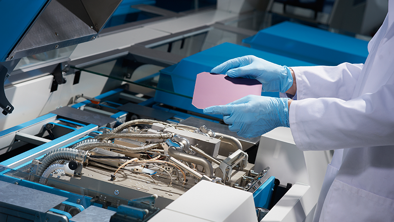
Sentech and SolayTec – a TNO spin-off – have been cooperating with one another in the development of atomic layer deposition (ALD) machines since 2012. This nanotechnology, which was optimized by SolayTec, enables manufacturers to produce solar cells with a higher output.
Higher output from solar cells thanks to ALD
As SolayTec’s R&D partner, Sentech developed sensor solutions to adequately monitor the ALD process performed by the machinery – solutions which rival sensor suppliers were unable to provide within SolayTec’s budget. The two firms based in the Dutch province of Brabant have since proceeded to supply this splendid example of precision mechanics worldwide.
ALD is a deposition technology which is used to apply layers at an atomic level. A substrate is exposed to sequential gas phase chemical processes. The chemical reactions that occur during exposure deposit a layer that is exactly the thickness of a single atom.
The cycle is then repeated until the desired layer thickness is achieved. ALD offers one particular advantage in this regard: it is a self-limiting process, as the chemical reaction halts as soon as the surface is covered. This makes for amazingly accurate control of both the layer thickness and homogeneity of the material.
Although ALD was invented quite some time ago, the technology was too laborious and expensive to be applied on an industrial scale. This recently changed, however, thanks to the efforts of the Netherlands Organization for Applied Scientific Research (TNO). In 2008, it launched a research project aimed at rendering ALD significantly quicker.
At the time, a number of other institutes, including the Eindhoven University of Technology, began publishing findings which showed that a thin layer of aluminum oxide applied to silicon solar cells using ALD produced substantially improved output.
“A nice homogeneous aluminum oxide film is vital to achieving the optimum effect,” SolayTec’s CTO, Ronald van Dijk, explains. The average solar panel has an efficiency level of around 18% to 20%. The application of aluminum oxide in the form of an extremely thin ALD film raises the overall output of a solar cell by more than 1%. This amounts to a relative increase of 5% to 7%.
ALD machine processes 4,000 wafers per hour
In 2009, TNO made a breakthrough that would enable solar cell manufacturers to benefit from the performance enhancing application of an ALD layer of aluminum oxide to their products: the spatial ALD process developed by the research institute make it possible to apply the film swiftly yet highly accurately.
Until then, TNO had simply been applying the standard temporal ALD process, whereby the substrate is exposed to the various gases in one room. Spatial ALD enabled it to shorten the rinsing phase by a factor of one thousand.
The resulting single cycle, in which the silicon solar wafer is conveyed contact-free through a series deposition units, takes just a few milliseconds instead of the previous six seconds.
In the first unit, the precursor gas, trimethyl aluminum (TMA), forms half the initial monolayer. In the next unit, water vapor completes the layer due to a chemical reaction between the TMA and water.
The process in the deposition unit can then be repeated several times to achieve the required thickness. Curtains of inert nitrogen gas between the deposition units prevent the precursor gases from coming into contact with one another.
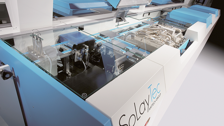
TNO’s research culminated in the installation of a patented deposition head in a prototype ALD machine in 2010. “This breakthrough placed a business case within reach,” Mr. Van Dijk explains. “In 2010, the spin-off firm SolayTec was founded with a view to marketing the TNO invention together with the prototype ALD machine.”
Mr. Van Dijk says that the challenge faced at that time was to wring more electric power out of an identical solar cell at equivalent cost. “The hectic start-up phase led to the introduction of the first production machine which had one deposition unit. We went on to further develop it into a machine comprising several deposition units, which can currently process up to four thousand wafers an hour.”
While SolayTec has customers throughout the world, the greatest demand for its machines is from China. Mr. Van Dijk: “The solar energy market is a growth market, which is sensitive to economic fluctuations. China has both energy and pollution problems, despite mass producing solar panels for the rest of the world.”
Sentech was the only party capable of meeting SolayTec’s sensor requirements. Erik Kremers, system architect at SolayTec, explains how Sentech became a candidate: “Our initial machine contained a number of motion sensors, with which to monitor the progress of the wafer through the deposition unit. The sensor that we were using for this purpose did not fully comply with our requirements in terms of both reliability and cost price, however. Reliable measurement of the wafer position within the sealed deposition unit, at a temperature of 200 degrees Celsius, is absolutely vital to the performance and uptime of our machines. If the wafer fails to proceed according to the set point, this can lead to breakdowns and damage, which then forces our customers to cease production. Downtime costs our customers money, of course.”
The sensor measures the edge of the wafer as it passes various points in the deposition unit. The measurement data acquired in this manner enables SolayTec to adjust the position of the wafer using software, so that it complies with the desired set point. Mr. Kremers: “We compiled specifications for a new sensor, which we then presented to both our existing and other sensor suppliers. However, none proved capable of supplying such a sensor within our budget. Then, Sentech suddenly popped up.”
Peter Verstappen, Sentech Account Manager, then organized roundtable talks with SolayTec, with a view to entirely developing a cost-effective sensor solution from scratch. Mr. Verstappen: “Sentech is an expert in the field of sensor integration and the development of sensor solutions. We like to sit down with customers first, to establish their concrete requirements. You won’t find what SolayTec needed in any sensor catalogue. SolayTec basically required an R&D partner. The technology was not the problem, but the price at which the sensor solution was to be supplied. Too high a sensor price would render the ALD machine too expensive to achieve the efficiency benefits envisaged by solar panel manufacturers.”
Temperature and cost price – the greatest challenges
Mr. Verstappen admits that the high temperature in the deposition unit posed the greatest challenge. Within just a few months of open cooperation with SolayTec, Sentech nevertheless succeeded in integrating an entirely new sensor solution in the first generation deposition unit in keeping with the envisaged production budget.
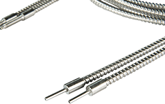
It was dubbed the DU 1.0. This optical positioning sensor comprises a glass fiber transmitter and amplifier, which transmit a beam of red light to a receiver. Digital detection is carried out at various points, where the edge of the wafer is measured as it passes the sensor, interrupting the light beam, and this provides 11 measurement readings.
Mr. Van Dijk proudly admits that, in supplying the DU 1.0, Sentech met SolayTec’s R&D requirements for its production machines to the latter’s complete satisfaction. “However, SolayTec wanted more,” Mr. Kremers continues.
“I still harbored the wish to incorporate a sensor that could monitor the wafer position continuously, instead of only at the existing discrete points. We would have much preferred to have a linear sensor that can monitor the entire 200-millimeter cycle of the wafer within the deposition unit. When I outlined this idea during a brainstorming session, Peter Verstappen did not immediately reject it as wishful thinking. Sentech fully comprehended my eagerness to closely monitor the position of the wafer: in order to improve the reliability of future models.”
Co-research & development yields scoping sensor that improves ALD machine reliability
“Digital detection using the DU 1.0 does have its limitations, as the sensor only takes a few readings. We therefore started experimenting with analogue signaling, as this enables one to determine positions within the space. This resulted in a scoping sensor, which can also monitor lateral movement, in complement to the positioning sensor. The combined readings of the two sensors provide a spatial impression of the wafer’s progress through the deposition unit.”
Mr. Kremers agrees that this solution comes pretty close to meeting his original wishes. “The new version offers a wealth of further information, which helps us proceed a few more steps.”
Messrs. Kremers and Van Dijk greatly appreciate Sentech’s frankness with regard to its development process.
Mr. Van Dijk: “We literally carry out open innovation together. The success of co-research & development is determined by the partners’ sincerity and willingness to share R&D insights. And both Sentech and SolayTec have cultures based on this kind of open attitude.”
The way of working for successful sensor integration
During a sensor integration project, you always weigh three interests: cost, quality and delivery time. What are the risks and consequences of my choice? Is the technology I have in mind the right solution for my application?
Scroll down our e-book for the answers to these questions. You can also read examples of common sensor issues and solutions.
Grant yourself this knowledge and download it for free.

